Graphite slicing yield is the percentage of raw billet material that becomes usable finished wafers after slicing. It is the single most important metric for evaluating slicing efficiency — and the one that directly connects process quality to production cost. A typical graphite slicing yield ranges from 45% to 80%, meaning 20–55% of the billet you purchased ends up as waste. The gap between a poorly optimized and well-optimized slicing operation can mean hundreds of extra wafers per shift from the same raw material input.
What Is Graphite Slicing Yield?
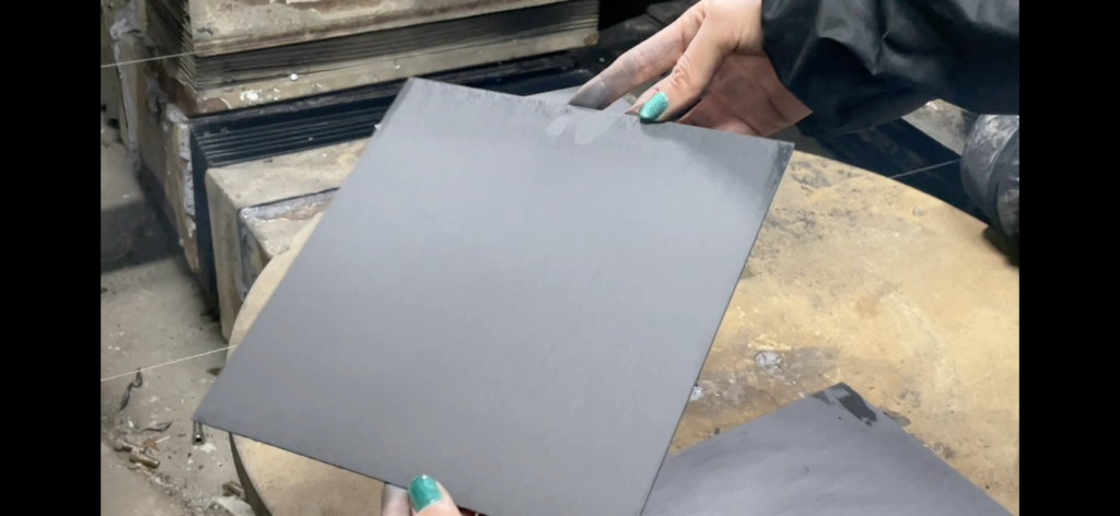
Graphite slicing yield is the ratio of total usable wafer volume to original billet volume, expressed as a percentage. A wafer is “usable” only if it meets all dimensional and quality specifications — thickness, TTV (total thickness variation), flatness, surface integrity, and freedom from cracks or chips.
Graphite slicing yield (%) = (Number of good wafers × Wafer volume) / Original billet volume × 100
Yield loss comes from four sources:
- Kerf loss — material destroyed by the cutting element (kerf loss guide)
- End trims — unusable material at both ends of the billet
- Scrap wafers — wafers that fail quality specs (cracks, chipping, out-of-tolerance thickness)
- Subsurface damage allowance — extra thickness added per wafer to allow post-slicing lapping
A complete yield improvement strategy must address all four sources, not just kerf.
흑연 슬라이싱 수율 — 주요 요인 및 그 영향
| 수율 요인 | 일반적인 손실 | Controllable? | 주요 개선 조치 |
|---|---|---|---|
| Kerf loss | 빌렛 18–45% | Yes — wire/blade selection | 더 얇은 다이아몬드 와이어 사용 (0.20–0.25 mm) |
| End trims | 빌렛 끝단당 2–5 mm | Partially — billet sizing | 목표 웨이퍼 수에 맞게 빌렛 길이 조정 |
| 스크랩률 (균열/칩) | 슬라이스된 웨이퍼 2–15% | 예 — 공정 매개변수 | 공급 속도 + 냉각수 + 장력 최적화 |
| TTV/평탄도 불량 | 슬라이스된 웨이퍼 1–8% | 예 — 장비 유지보수 | 가이드, 장력, 고정구 정렬 보정 |
| Lapping allowance | 0.02–0.10 mm per face | Partially — depends on as-cut quality | 슬라이싱 스트레스 감소 → 래핑 필요량 감소 |
Key insight: Kerf loss gets the most attention, but scrap rate and lapping allowance combined can exceed kerf loss in poorly controlled operations. A 5% scrap rate on expensive isostatic graphite wafers is often more costly than 2% extra kerf loss.
How to Improve Graphite Slicing Yield: Step-by-Step
Step 1: Minimize Kerf Loss Through Wire Selection
The most impactful yield improvement. Switching from ID saw (0.5–0.8 mm kerf) to diamond wire (0.20–0.25 mm kerf) can increase wafer output by 25–35% per billet.
For operations already using diamond wire, evaluate:
- Can you move to a thinner wire diameter? (0.25 mm → 0.20 mm = ~20% kerf reduction)
- Is wire quality consistent? Inconsistent diamond coating causes variable kerf width
- Are you replacing wire at the optimal interval? Worn wire increases kerf through deflection
Refer to our detailed kerf loss reduction guide for parameter-level optimization.
Step 2: Reduce Scrap Rate by Controlling Cutting Defects
Every cracked, chipped, or warped wafer is a direct yield loss — the material, machine time, and wire used to produce it are all wasted. The most common defects and their fixes:
Edge chipping: Usually caused by excessive feed rate or graphite grain size mismatch with wire grit. Reduce feed rate by 15–20% and verify your diamond grit is appropriate for the material’s grain structure. Fine-grained isostatic graphite (≤10 μm) tolerates faster feed than coarse extruded grades.
Wafer cracking: 과도한 슬라이싱 스트레스로 인해 발생 — 너무 많은 절단력, 열 충격 또는 고정 장치로 인한 사전 응력. 빌렛 마운팅 접착제의 균일성을 확인하고, 공급 속도를 줄이며, 냉각수가 전체 절단 영역에 도달하는지 확인하십시오.
Surface waviness: Wire deflection during cutting creates an uneven surface. Tighten wire tension within specification, inspect guide rollers for wear, and reduce feed rate. Wavy surfaces increase lapping allowance requirements, compounding yield loss.
For a comprehensive defect catalog, see our slicing defects guide.
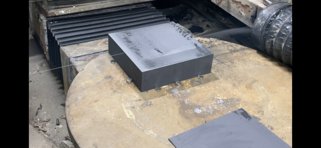
Step 3: Optimize Billet Utilization
End trims and sizing waste are often overlooked:
- Match billet length to wafer count. Calculate the optimal billet length as: (target wafer thickness + kerf width) × desired wafer count + end trim allowance. Order billet lengths that minimize leftover material.
- Minimize end trim allowance. End trims compensate for billet face irregularity and initial wire engagement instability. A well-prepared billet face (ground flat before slicing) reduces the end trim from 3–5 mm to 1–2 mm per end.
- Reuse offcuts. End trims and undersized pieces from one billet can sometimes be combined with offcuts from other billets for secondary products or test wafers.
Step 4: Tighten Thickness Control to Reduce Lapping Allowance
래핑 여유량은 최종 웨이퍼가 슬라이싱 후 표면 보정 후 사양을 충족하도록 보장하기 위해 각 웨이퍼의 목표 두께에 추가되는 추가 재료입니다. 두께 제어가 양호한 경우(TTV 0.05 mm)에는 면당 0.05–0.10 mm가 필요합니다. 이는 래핑에서 소비되는 재료가 제품으로 제공되는 것보다 웨이퍼당 0.06–0.14 mm 더 추가되는 것입니다.
Over hundreds of wafers per billet, reducing lapping allowance from 0.10 mm to 0.03 mm per face recovers material equivalent to several additional wafers.
Step 5: Implement Statistical Process Monitoring
Track these metrics per production batch:
- Wafers per billet — the headline yield number. Plot as a trend chart.
- Scrap rate by defect type — identifies which specific problem to fix first
- TTV distribution — histogram showing how tightly your process controls thickness
- Kerf width trend — rising kerf indicates wire wear or equipment drift
When yield drops, these metrics tell you exactly where to look. Without data, yield improvement becomes guesswork.
Graphite Slicing Yield Troubleshooting
Yield Dropping Gradually Over Weeks — What to Do?
Check wire quality and equipment wear systematically. Gradual yield decline usually means a slow-moving variable is drifting: guide roller wear (increases kerf width and TTV), coolant contamination (increases scrap from defects), or wire quality variation between batches. Compare current kerf width and scrap rate against your baseline. The metric that changed first points to the root cause.
Yield Suddenly Drops on a Specific Graphite Grade?
The material properties changed — not your machine. Different production lots of the same graphite grade can vary in density, grain size distribution, and binder content. Request the material certificate for the new lot and compare to previous lots. If grain size is coarser, reduce feed rate by 10–20%. If density is lower, check for increased porosity that may cause subsurface chipping.
High Yield but Many Wafers Failing Post-Slicing QC?
Your slicing yield looks good but downstream yield is low — meaning wafers pass visual inspection at the saw but fail dimensional or surface quality checks later. This typically indicates that your in-process inspection criteria are too loose. Tighten the pass/fail threshold at the saw to catch marginal wafers before investing lapping time in them. Also check flatness and parallelism measurement accuracy — a miscalibrated gauge gives false passes.
Yield Varies Significantly Between Operators?
Standardize the setup procedure. Yield variation between operators means the process depends on individual technique rather than documented parameters. Create a setup checklist covering: billet mounting adhesive application, wire tension verification, feed rate setting, coolant flow confirmation, and first-wafer inspection criteria. Train all operators to the same standard and audit compliance monthly.
Graphite Slicing Yield vs Silicon Wafer Yield: How They Compare
| Factor | Graphite Slicing | Silicon Wafer Slicing |
|---|---|---|
| Typical yield | 45–80% | 50–85% |
| Material cost impact | Moderate-high (isostatic graphite) | Very high (single crystal silicon) |
| Primary yield limiter | Kerf loss + scrap (brittleness) | Kerf loss + TTV |
| Grain structure | Polycrystalline (variable grain) | Single crystal (uniform) |
| Chipping risk | High (brittle, grain boundaries) | Moderate (cleavage planes) |
| Typical kerf (diamond wire) | 0.20–0.30 mm | 0.15–0.20 mm |
| Post-slicing lapping | Common | Almost always |
| Yield monitoring maturity | Often informal | Highly instrumented |
Graphite slicing can learn from silicon wafer manufacturing’s emphasis on statistical process control and equipment calibration discipline. The same principles apply — graphite operations just tend to implement them less rigorously.
How Endless Diamond Wire Cutting Improves Graphite Slicing Yield
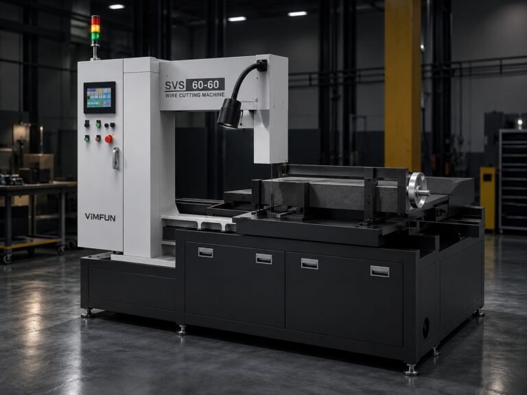
Endless (loop) diamond wire cutting addresses the key yield loss factors through precision single-wire control:
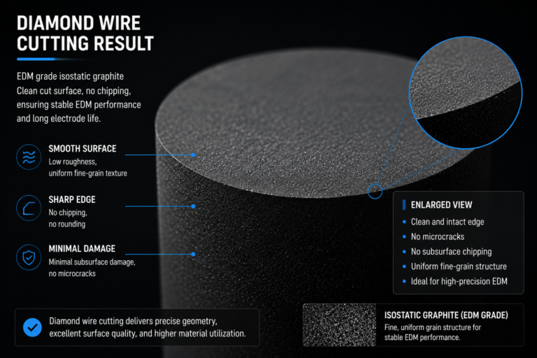
Narrow kerf: Endless diamond wire with diameters of 0.30–0.50 mm produces significantly narrower kerf than traditional ID saw blades (0.5–0.8 mm), increasing the number of usable wafers per billet.
Consistent wire condition: Unlike open-wire systems where the wire degrades progressively from spool start to end, an endless diamond wire loop maintains consistent abrasive condition throughout the cut. This produces uniform kerf width and surface quality across every slice, reducing scrap from inconsistent cutting.
Flexible workpiece handling: Single-wire loop cutting accommodates a wide range of billet sizes and shapes without retooling. This flexibility allows operators to optimize billet orientation for maximum yield — cutting along the longest dimension to minimize end trim waste.
Lower cutting force: 연속 루프 설계는 일정한 와이어 장력과 속도를 유지하여 ID 톱보다 낮은 절단력을 생성합니다. 이는 슬라이싱 스트레스를 줄이고, 더 얕은 표면하 손상을 생성하며, 절단 후 필요한 래핑 여유량을 최소화합니다.
In our graphite slicing applications, customers switching from ID saw to endless diamond wire cutting typically see:
- Graphite slicing yield improvement through narrower kerf and lower scrap rate
- Reduced edge chipping due to lower cutting forces
- More consistent thickness across production runs
The specific yield improvement depends on your graphite grade, current equipment, and wafer specifications. For a detailed assessment, see our 정밀 흑연 슬라이싱 overview or contact our engineering team with your current billet dimensions and yield data.