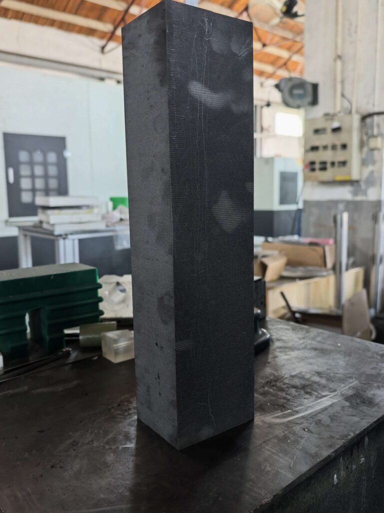
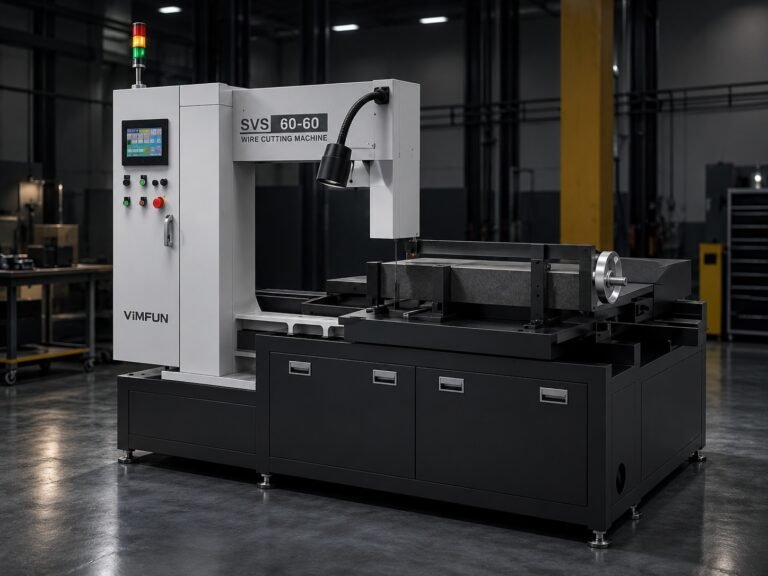
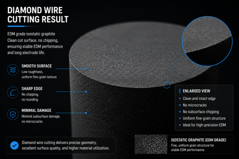
グラファイトスライシング歩留まりとは、スライス後に使用可能な完成ウェーハになる生のビレット材料の割合です。これは、スライシング効率を評価する上で最も重要な指標であり、プロセス品質と生産コストを直接結びつけるものです。典型的なグラファイトスライシング歩留まりは45%から80%の範囲であり、購入したビレットの20%から55%が廃棄物となることを意味します。スライシング操作の最適化が不十分な場合と最適化が十分な場合では、同じ原材料投入量からシフトあたり数百枚の追加ウェーハが得られる可能性があります。.
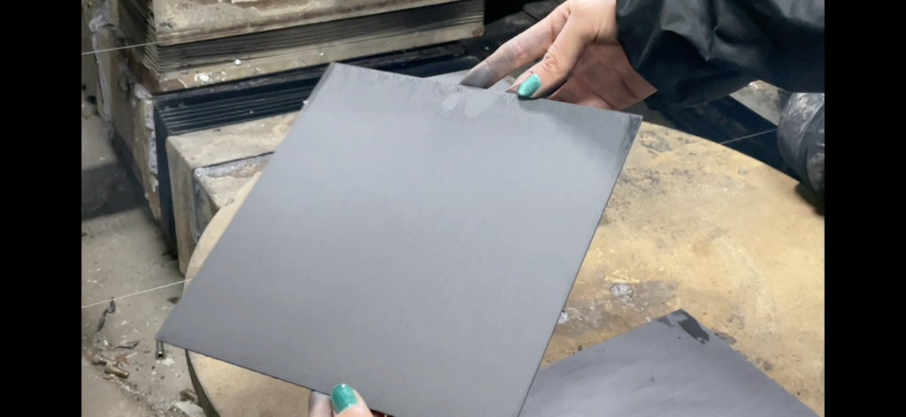
グラファイトスライシング歩留まりとは何ですか?
グラファイトスライシング歩留まりとは、総使用可能ウェーハ体積と元のビレット体積の比率をパーセンテージで表したものです。ウェーハは、厚さ、TTV(総厚さ変動)、平坦度、表面完全性、およびひび割れや欠けがないというすべての寸法および品質仕様を満たしている場合にのみ「使用可能」です。.
グラファイトスライシング歩留まり (%) = (良品ウェーハ数 × ウェーハ体積) / 元のビレット体積 × 100
歩留まり損失は4つの原因から生じます。
- カーフ損失 — 切断要素によって破壊された材料(カーフ損失ガイド)
- 端部トリム — ビレットの両端の未使用材料
- スクラップウェーハ — 品質仕様を満たさないウェーハ(ひび割れ、欠け、許容範囲外の厚さ)
- サブサーフェスダメージ許容値 — スライス後のラップを可能にするためにウェーハごとに追加される厚さ
完全な歩留まり改善戦略は、カーフだけでなく、これら4つの原因すべてに対処する必要があります。.
グラファイトスライシング歩留まり — 主要因とその影響
| 歩留まり要因 | 一般的な損失 | 制御可能か? | 主要な改善策 |
|---|---|---|---|
| カーフ損失 | ビレット18〜45% | はい — ワイヤー/ブレードの選択 | より細いダイヤモンドワイヤー(0.20〜0.25 mm)を使用する |
| 端部トリム | ビレット端あたり2〜5 mm | 部分的に — ビレットサイジング | 目標ウェーハ数に合わせてビレット長を調整する |
| スクラップ率(ひび割れ/欠け) | スライスウェーハの2〜15% | はい — プロセスパラメータ | 送り速度 + クーラント + 張力を最適化する |
| TTV/平坦度不良 | スライスウェーハの1〜8% | はい — 装置メンテナンス | ガイド、張力、治具のずれを校正する |
| Lapping allowance | 面あたり 0.02~0.10 mm | Partially — depends on as-cut quality | Reduce slicing stress → less lapping needed |
Key insight: Kerf loss gets the most attention, but scrap rate and lapping allowance combined can exceed kerf loss in poorly controlled operations. A 5% scrap rate on expensive isostatic graphite wafers is often more costly than 2% extra kerf loss.
How to Improve Graphite Slicing Yield: Step-by-Step
Step 1: Minimize Kerf Loss Through Wire Selection
The most impactful yield improvement. Switching from ID saw (0.5–0.8 mm kerf) to diamond wire (0.20–0.25 mm kerf) can increase wafer output by 25–35% per billet.
For operations already using diamond wire, evaluate:
- Can you move to a thinner wire diameter? (0.25 mm → 0.20 mm = ~20% kerf reduction)
- Is wire quality consistent? Inconsistent diamond coating causes variable kerf width
- Are you replacing wire at the optimal interval? Worn wire increases kerf through deflection
Refer to our detailed kerf loss reduction guide for parameter-level optimization.
Step 2: Reduce Scrap Rate by Controlling Cutting Defects
Every cracked, chipped, or warped wafer is a direct yield loss — the material, machine time, and wire used to produce it are all wasted. The most common defects and their fixes:
Edge chipping: Usually caused by excessive feed rate or graphite grain size mismatch with wire grit. Reduce feed rate by 15–20% and verify your diamond grit is appropriate for the material’s grain structure. Fine-grained isostatic graphite (≤10 μm) tolerates faster feed than coarse extruded grades.
Wafer cracking: Caused by excessive slicing stress — too much cutting force, thermal shock, or fixture-induced pre-stress. Check billet mounting adhesive for uniformity, reduce feed rate, and verify coolant reaches the full cutting zone.
Surface waviness: Wire deflection during cutting creates an uneven surface. Tighten wire tension within specification, inspect guide rollers for wear, and reduce feed rate. Wavy surfaces increase lapping allowance requirements, compounding yield loss.
For a comprehensive defect catalog, see our slicing defects guide.
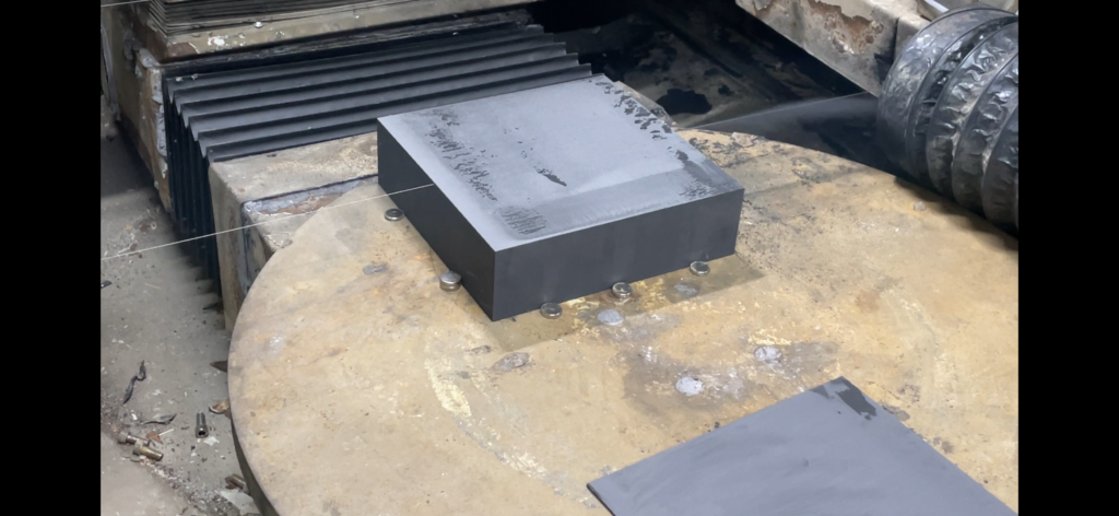
Step 3: Optimize Billet Utilization
End trims and sizing waste are often overlooked:
- Match billet length to wafer count. Calculate the optimal billet length as: (target wafer thickness + kerf width) × desired wafer count + end trim allowance. Order billet lengths that minimize leftover material.
- Minimize end trim allowance. End trims compensate for billet face irregularity and initial wire engagement instability. A well-prepared billet face (ground flat before slicing) reduces the end trim from 3–5 mm to 1–2 mm per end.
- Reuse offcuts. End trims and undersized pieces from one billet can sometimes be combined with offcuts from other billets for secondary products or test wafers.
Step 4: Tighten Thickness Control to Reduce Lapping Allowance
Lapping allowance is the extra material added to each wafer’s target thickness to ensure the finished wafer meets specification after post-slicing surface correction. If your thickness control is good (TTV 0.05 mm) requires 0.05–0.10 mm per face — an additional 0.06–0.14 mm of material per wafer consumed in lapping rather than delivered as product.
Over hundreds of wafers per billet, reducing lapping allowance from 0.10 mm to 0.03 mm per face recovers material equivalent to several additional wafers.
Step 5: Implement Statistical Process Monitoring
Track these metrics per production batch:
- Wafers per billet — the headline yield number. Plot as a trend chart.
- Scrap rate by defect type — identifies which specific problem to fix first
- TTV distribution — histogram showing how tightly your process controls thickness
- Kerf width trend — rising kerf indicates wire wear or equipment drift
歩留まりが低下した場合、これらの指標はどこを確認すべきかを正確に示します。データがなければ、歩留まりの改善は推測になります。.
グラファイトスライシング歩留まりトラブルシューティング
数週間にわたって徐々に歩留まりが低下した場合 — どうすればよいですか?
ワイヤーの品質と装置の摩耗を体系的に確認してください。徐々に歩留まりが低下する場合は、通常、ゆっくりと変化する変数がドリフトしていることを意味します。ガイドローラーの摩耗(カーフ幅とTTVを増加させる)、クーラントの汚染(欠陥によるスクラップを増加させる)、またはバッチ間のワイヤー品質のばらつきです。現在のカーフ幅とスクラップ率をベースラインと比較してください。最初に変化した指標が根本原因を示します。.
特定のグラファイトグレードで歩留まりが突然低下した場合?
材料の特性が変化した — 機械ではありません。同じグラファイトグレードでも、生産ロットが異なると、密度、粒度分布、およびバインダー含有量が異なる場合があります。新しいロットのマテリアル証明書を要求し、以前のロットと比較してください。粒度が粗い場合は、送り速度を10〜20%削減してください。密度が低い場合は、サブサーフェスチッピングを引き起こす可能性のある気孔率の増加を確認してください。.
歩留まりは高いが、スライシング後のQCで多くのウェーハが不合格になる場合?
スライシングの歩留まりは良好ですが、下流の歩留まりが低い — これは、ウェーハがソーでの目視検査に合格しても、後で寸法または表面品質のチェックに失敗することを意味します。これは通常、インプロセス検査基準が緩すぎることを示しています。ラッピング時間を投資する前に、ソーでの合格/不合格のしきい値を厳しくして、限界的なウェーハを捕捉してください。また、 flatness and parallelism 測定精度を確認してください — 校正されていないゲージは誤った合格を与えます。.
オペレーター間で歩留まりが大きく変動する場合?
セットアップ手順を標準化してください。オペレーター間の歩留まりのばらつきは、プロセスが文書化されたパラメータではなく、個々の技術に依存していることを意味します。次の項目をカバーするセットアップチェックリストを作成してください。ビレットマウント接着剤の塗布、ワイヤー張力の検証、送り速度の設定、クーラントフローの確認、および最初のウェーハの検査基準。すべてのオペレーターを同じ基準でトレーニングし、毎月コンプライアンスを監査してください。.
グラファイトスライシング歩留まり vs シリコンウェーハ歩留まり:比較方法
| 要因 | グラファイトスライシング | シリコンウェーハスライシング |
|---|---|---|
| 通常の歩留まり | 45–80% | 50–85% |
| Material cost impact | Moderate-high (isostatic graphite) | Very high (single crystal silicon) |
| Primary yield limiter | Kerf loss + scrap (brittleness) | Kerf loss + TTV |
| Grain structure | Polycrystalline (variable grain) | Single crystal (uniform) |
| Chipping risk | High (brittle, grain boundaries) | Moderate (cleavage planes) |
| Typical kerf (diamond wire) | 0.20–0.30 mm | 0.15–0.20 mm |
| Post-slicing lapping | Common | Almost always |
| Yield monitoring maturity | Often informal | Highly instrumented |
Graphite slicing can learn from silicon wafer manufacturing’s emphasis on statistical process control and equipment calibration discipline. The same principles apply — graphite operations just tend to implement them less rigorously.
How Endless Diamond Wire Cutting Improves Graphite Slicing Yield
Endless (loop) diamond wire cutting addresses the key yield loss factors through precision single-wire control:
Narrow kerf: Endless diamond wire with diameters of 0.30–0.50 mm produces significantly narrower kerf than traditional ID saw blades (0.5–0.8 mm), increasing the number of usable wafers per billet.
Consistent wire condition: Unlike open-wire systems where the wire degrades progressively from spool start to end, an endless diamond wire loop maintains consistent abrasive condition throughout the cut. This produces uniform kerf width and surface quality across every slice, reducing scrap from inconsistent cutting.
Flexible workpiece handling: Single-wire loop cutting accommodates a wide range of billet sizes and shapes without retooling. This flexibility allows operators to optimize billet orientation for maximum yield — cutting along the longest dimension to minimize end trim waste.
Lower cutting force: The continuous loop design maintains steady wire tension and speed, generating lower cutting forces than ID saws. This reduces slicing stress, produces shallower subsurface damage, and minimizes the lapping allowance needed after cutting.
In our graphite slicing applications, customers switching from ID saw to endless diamond wire cutting typically see:
- Graphite slicing yield improvement through narrower kerf and lower scrap rate
- Reduced edge chipping due to lower cutting forces
- More consistent thickness across production runs
The specific yield improvement depends on your graphite grade, current equipment, and wafer specifications. For a detailed assessment, see our 精密グラファイトスライス overview or contact our engineering team with your current billet dimensions and yield data.